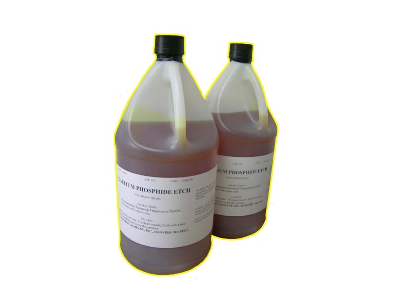
GALLIUM PHOSPHIDE ETCHANT GaP
TRANSENE Gallium Phosphide Etchant is an effective etchant designed for the fabrication of light emitting diodes and diode matrix arrays. It offers controlled chemical etching of gallium phosphide to produce mesa structures, required for efficient LED and for the separation of LED to generate matrix arrays of alpha numeric displays.
During the separation the LED can be shaped into domed structures, also essential for efficient electroluminescent devices. The etchant is, furthermore, compatible with lead beam technology.
TRANSENE Gallium Phosphide Etchant exhibits a high etch rate for all crystal orientations. All crystal faces of the <100> orientation of GaP are etched uniformly, producing a polished unpitted surface.
The faces of the <111> orientation etch dirrerently; the <111> (Ga plane A face) develops a smooth orange-peel surface, whereas the <111> (P plane B face) becomes smooth, polished and unpitted. N- and P-type GaP have equivalent etch rates.
GaP Etchant is a stable, economical formulation based on potassium hexacyanoferrate and easily used for state-fo-the-art gallium phosphide LED and beam lead electroluminescent devices. The etchant does not attack Pd, Au or Pt lead beam metallizations. Ti and SiO2 masks show minimal attack. GaP Etchant is also effective for SiC and GaN applications.
PROPERTIES :
| | Gallium Phosphide Etchant GaP
|  |
| Appearance | Amber liquid |
| Operating Temperature | 70 ~ 80℃ |
| Solvent Rinse | H2O |
| pH | 13 - 14 |
| Tank | Glass or polypropylene |
| Etch Rate @ 80℃ in Microns/hour | P-type <100> | 210 |
| N-type <100> | 210 |
| P-type <111> | --- |
| A face (Gallium) | 115 |
| B face (Phosphorus) | 210 |
Etch Capacity
| 12 grams/liter |
Compatible Beam Lead Materials
| Ti, Pd, Au, Cr, Pt |
| Compatible Dielectric Material | Sputtered or Silane SiO2 |
| Compatible Masking Material | SiO2, Ti, Au, KMER |
APPLICATION :
TRANSENE Gallium Phosphide Etchant is employed in several manufacturing operations for the production of light emitting diodes. The etchant may be used first to remove surface damage of mechanically polished p-type and n-type gallium phosphide. The following procedures are generally followed for device fabrication :
• Formation of mesa configuration with GaP etchant and SiO2 as a mask.
• Beam lead metallization and contact metallizations using photoresist techniques.
• Separation of GaP wafer into individual die, by partial cutting with abrasive dicing machines followed by chemical etching with TRANSENE GaP Etchant.
PACKAGING :
• Custom packaging is available upon request.