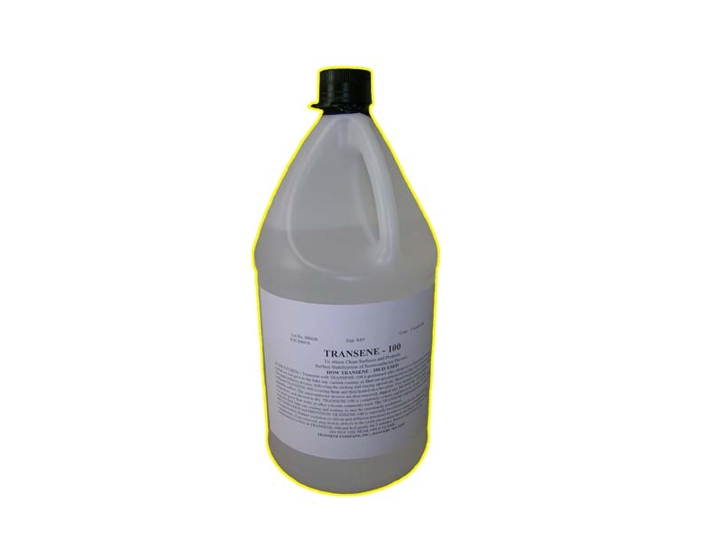
Ultra Clean Surfaces TRANSENE 100
FEATURES :
• Stabilization of semiconductor devices through clean surfaces
• Overcomes soft reverse characteristics when due to surface contaminants
• Generates higher yield of p-n juncton devices.
• Useful for final cleaning process before thermal oxidation of silicon, diffusion and after p-n junction etches.
What is TRANSENE-100
TRANSENE-100 is a new chemical product designed for use in the semiconductor industry, to improve quality, yields, and reliability of p-n junction devices. It is especially applicable to transistors, diodes, rectifiers, and intergrated circuits. TRANSENE-100 serves to establish clean surfaces and ensure surface stabillization of semiconductor devices when it is properly used.
PROPERTIES :
| | TRANSENE-100
|  |
| Boiling Point Range | 75-101℃ |
| Specific Gravity | 0.75 |
| Heavy Metals | <0.35 ppm |
| Particulate matter | None (visually) |
| Acidity | Neutral |
| Flash Point | 21-24℃ |
| Contact Hazard | Very slight irritant, not dangerous |
| MAC | 400 parts per million |
| Fire Hazard | When exposed to flame |
| Ventilation Control | Normal ventilation rate, use of hood preferred |
| Spontaneous combustion | No |
| Toxic Hazard | Narcotic systemically |
How TRANSENE-100 Works :
The primary function of TRANSENE-100 is to remove foreign substance found on semiconductor surfaces. These substances may be loosely held on the surface or they may be absorbed electrolytes or precipitated metals. Water, alcohol, acetone, and other solvents fail to remove them efficiently or else not at all. TRANSENE-100 is efficient in breaking van der Waals forces responsible for tenacious binding of some foreign substances.
TRANSENE-100 is also capable of removing substances absorbed on semiconductor surfaces. In general, much surface contamination can be extracted by use of TRANSENE-100. This product, however, is not a chemical etch and is not intended as a substitute ofr chemical etching.
Why use TRANSENE-100 :
Surface cleanliness has a very special meaning in the manufacture of semiconductor products. The presence of foreign material at junction sites may lead to highly localized fields where current is drawn through by Zener tunneling, resulting in high reverse currents.
The occurrence, even in minute trace quantities, of ions, electrolytes, or metal impurities on semiconductor surfaces cause poor device electrical characteristics, such as hysteresis, flutter, and high leakage current. Mobile ions located anywhere on the active device surface will affect ultimate device reliability, particularly at high temperature operation. With TRANSENE-100 a relatively clean surface characterized by stable surface states is produced.
How TRANSENE-100 is used :
AFTER ETCHING - Treatment with Transene 100 is performed after chemical or electrolytic etching is carried out, but prior to the bakeout, varnish coating, or final encapsulation and sealing or p-n junction devices. The semiconductor devices, following the etching and rinsing operations, should be placed in a beaker with sufficient TRANSENE-100 covering them and then heated on a hot plate
Five minutes of gentle boiling generally suffice. The semiconductor devices are then removed TRANSENE-100 is completely volatile and leaves no residue. In this respect, it is much purer than water or other solvents commonly used.
The TRANSENE 100 treated devices are now ready for final bakeout, coating, and sealing, as may be customarily performed.
PRE OXIDATION and DIFFUSION- TRANSENE-100 is especially recommended for the final cleaning treatment before thermal oxidation of silicon and diffusion processes to remove surface contaminants. These contaminants if not removed may lead to pinholes in the oxide passivation layer and faulty diffusions.